PDF] Design and Fabrication of Bond Pads for Flip-Chip Bonding of

By A Mystery Man Writer
At the University of Alberta, the Imaging Science Lab aims to develop vertically-integrated (VI) CMOS image sensors with capabilities that exceed those of conventional CMOS image sensors. VI-CMOS image sensors are examples of 3D electronics because they consist of photodetectors that are placed in a layer above standard CMOS circuits. Although metal lines commonly pass over transistors in CMOS image sensors, a distinguishing characteristic of VI-CMOS image sensors is the layering of semiconductor devices. The main advantage of vertical integration is that the different layers may be fabricated using different processes, each one optimized to best suit the type of devices it contains.
Flip chip - Wikipedia

Flip Chip: 1 Process Steps, PDF, Manufactured Goods

Bonding process of the ACF flip chip package; (a) before bonding

Thermosonic fine-pitch flipchip bonding of silicon chips on screen

Digital Design
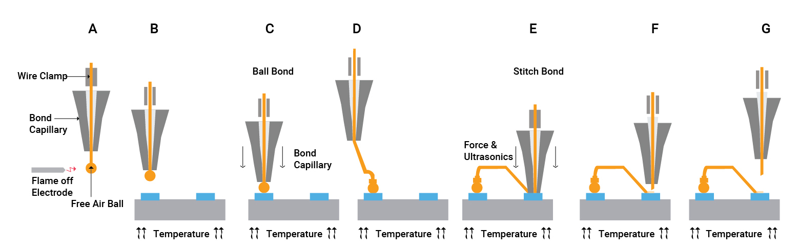
Wire Bonding: Efficient Interconnection Technique

III/V-on-Si MQW lasers by using a novel photonic integration
Electronics, Free Full-Text
Design guide - Mandalon EN

Proof of concept for through silicon vias in application-specific

Flip Chip technology
- Ebook & Journal
- pcb - Connecting pads with the same functionality belonging to one chip - Electrical Engineering Stack Exchange

- Anion Sanitary Napkins Sanitary Pad Ultra Thin

- Apple Not Giving iPad Wi-Fi Chip Orders To MediaTek, Says Analyst

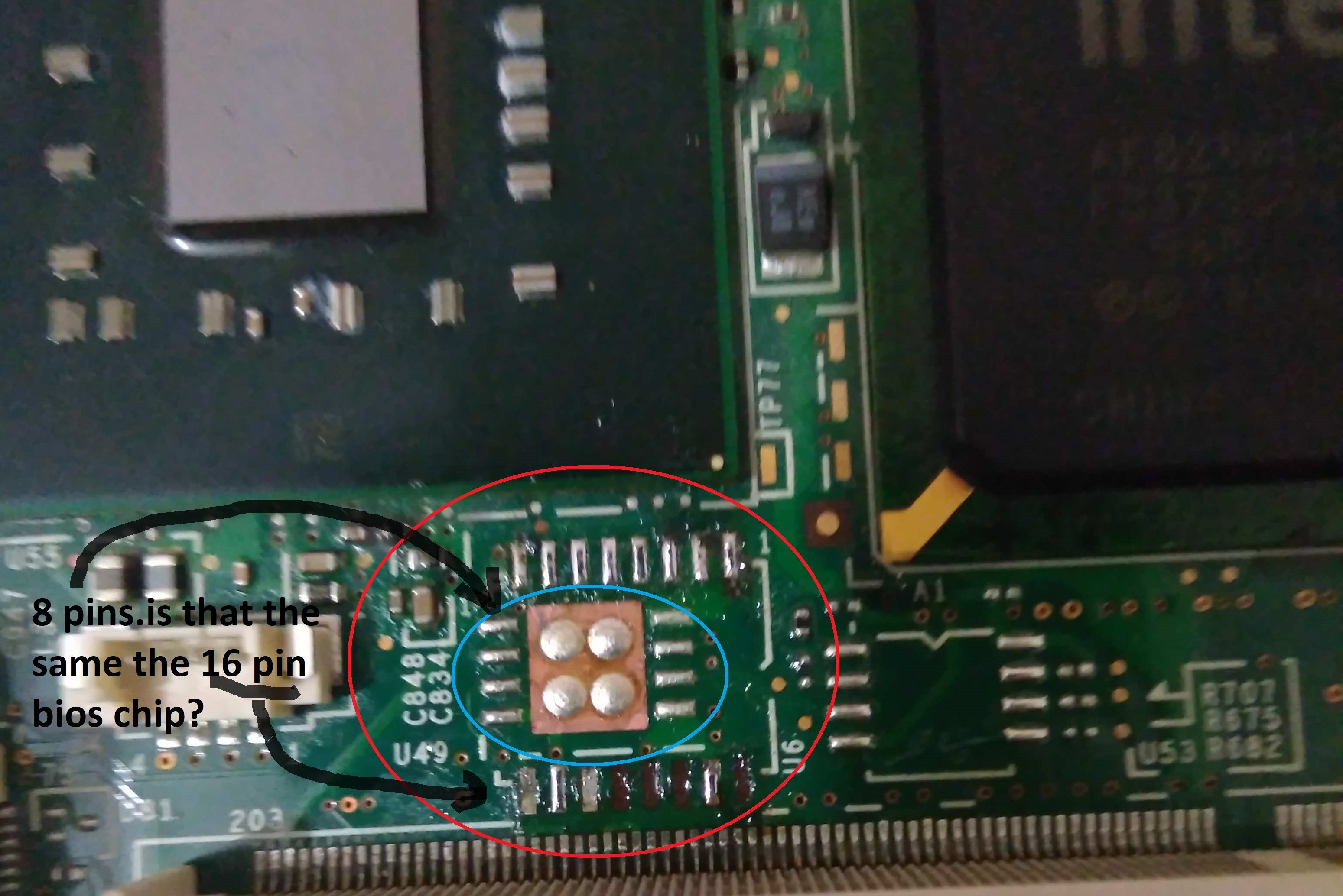
- t500-bios-chip-lifted-pad-issue - English Community - LENOVO COMMUNITY