Wednesday, Oct 02 2024
Bonding Pad Design Ⅱ
By A Mystery Man Writer
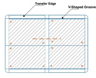
Cylindrical component bonding pad design - The shape of bonding pad is rectangle. When the reflow soldering process is applied, a concave groove must be designed

PDF] Active device under bond pad to save I/O layout for high-pin-count SOC

2 Layers Bonding Pads PCB Board, Standard PCB,Quickturn PCB,Bonding PCB
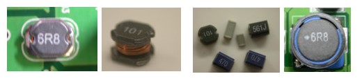
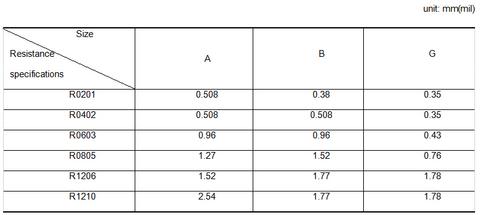
SMT Passive Parts (Reference Article)

Wire Bonding, a Way to Stitch Chips to PCBs - SK hynix Newsroom

Illustration in concept of a traditional bond pad structure, 4 levels
Bonding Pad Design Ⅱ
Printed Circuit Board Panel Design
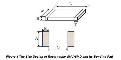
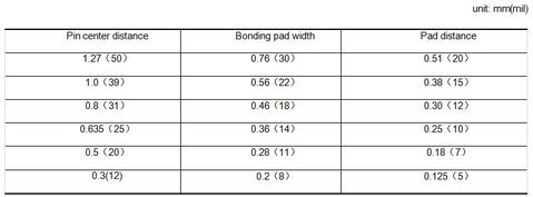
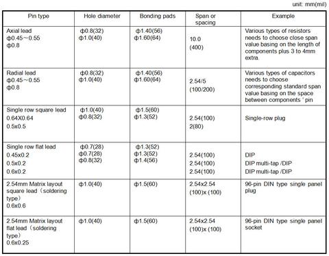
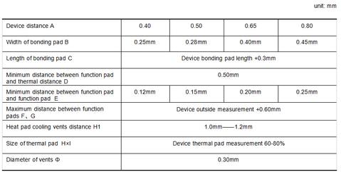
Design Requirement of SMT PCBs Part One: Bonding Pad Design of Some Ordinary Components

Bonding Pad - an overview
Bonding Pad Design Ⅰ
Bonding Pad Design Ⅱ
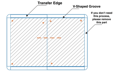
Printed Circuit Board Panel Design
Related searches

Related searches
- Just My Size Cotton White Briefs 6-Pack Underwear Panties Panty Women JMS Comfor

- Wacoal Women's Embrace Lace Underwire Bra, Black, 32B

- Alinhadores Invisalign em Guarulhos (11) 4378-0010

- Pull-Ups Learning Designs Boys' Potty Training Pants 4T-5T (38-50
- Supreme Light & Ultra Comfortable Wired Push Up Bra 01-1007


©2016-2024, travellemur.com, Inc. or its affiliates