The complete guide to PCB pad :types, size, spacing, repair and

By A Mystery Man Writer
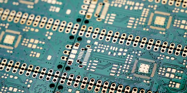
Soldering is one of the most important processes in PCBA processing. On printed circuit boards, electrical connections to all components are made via PCB pads. The PCB pads are a very critical part of the PCB that determines where components are soldered on the PCB.The size, shape, and position of pads in a PCB directly depend on the manufacturing quality of the board. Today we will take a look at the PCB pad in SMT soldering.
Soldering is one of the most important processes in PCBA processing. On printed circuit boards, electrical connections to all components are made via PCB pad.

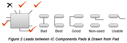
PCB Layout and The requirements of The Drawing of Pads - PCB Design & Layout - PCBway

PCB Etching : a guide to materials, methods, and safety precautions - IBE Electronics

PCB connector : definition, types, and how to choose and identify - IBE Electronics

What is reflow soldering? Technological process, defects and comparison with wave soldering - IBE Electronics
What is Pad to Pad (PP) in PCB ?. Pad to Pad or PP is an important design…, by RayMingPCB
What are Vias in Pad? Advantages, Limitations, Applications, and Comparison with Conventional Vias
Design Requirement of SMT PCBs Part Two: Settings of Pad-Trace Connection, Thru-Holes, Test Point, Solder Mask and Silkscreen

PCB Pad Size Guidelines: Finding the Proper Pad Sizes for Your Circuit Design

What is reflow soldering? Technological process, defects and comparison with wave soldering - IBE Electronics

PCB Pad Size Guidelines: Finding the Proper Pad Sizes for Your Circuit Design

What is a Pad in PCB Design and Development

Understanding solder joint - basics and techniques - IBE Electronics

- Faux Fur Scarf - Temu Canada

- Korean Long Puffer Coat - Best Price in Singapore - Mar 2024

- The Hidden Life and Tragic Final Days of Lt. Columbo Peter Falk

- My boobs are way too big. I'm thinking about a breast reduction

- Vintage Stonewash - BillrichardsonShops Stan Ray OG Denim Painter Pants - R13 Courtney Cropped-Jeans Blau
