Monday, Oct 07 2024
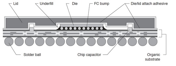
Schematic of the chip/bump build-up cross-section.
By A Mystery Man Writer
Package Substrate, SAMSUNG ELECTRO-MECHANICS

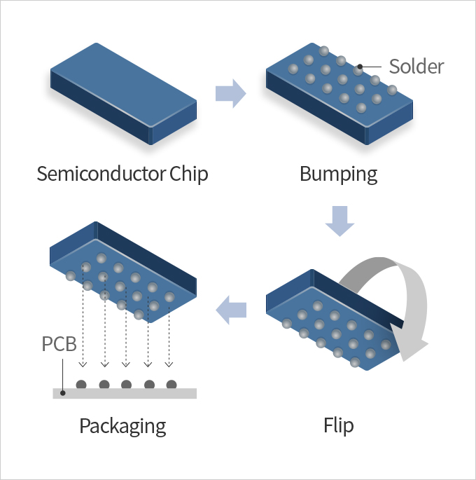
Advanced Flip Chip Packaging
A Brief Introduction of BGA Package Types

An efficient RDL routing for flip-chip designs - EDN
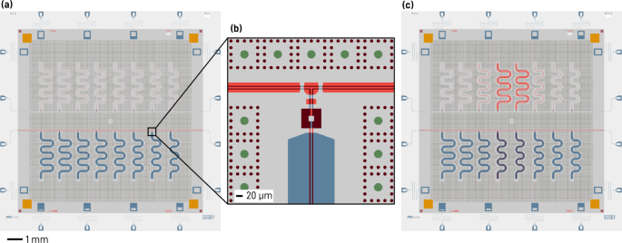
Improved parameter targeting in 3D-integrated superconducting

Scade One - A Visual Coding Experience - Ansys Knowledge

PDF) Understanding and Improving Reliability for Wafer Level Chip

Chiplets Lateral Communications

Schematic of the chip/bump build-up cross-section.
Challenges Grow For Creating Smaller Bumps For Flip Chips

Schematic of the chip/bump build-up cross-section.
Levels and Steps of Integration. Introduction, by Suny Li

PDF) Understanding and Improving Reliability for Wafer Level Chip

SEM image of a cross section of a flip-chip with 30 μm solder
Related searches
- Sensors, Free Full-Text

- Anion Sanitary Napkins Sanitary Pad Ultra Thin

- Thermal Adhesive Tape, 25m x 20mm x 0.2mm High Performance Double Side Thermal Tapes Cooling Pad Apply to Heatsink, LED, IGBT, IC Chip, Computer

- Chip Pad Bra Full - Medivaris

- Wire bonding from chip to bonding pads and connection to leadframe

Related searches


©2016-2024, travellemur.com, Inc. or its affiliates